Semiconductor
For semiconductor packaging, test and back-end process steps, providing visual inspection solutions for precision part presence/absence, position and appearance anomalies.
Industry Production characteristics
How This Industry Produces Determines How Inspection Should Be Done
The visual inspection of semiconductors revolves around two things: first, making the most common defects in this industry image clearly and consistently; second, connecting the judgement result reliably into the production line. Common implementation constraints in this industry are "inspection objects are extremely small and require high-magnification optical systems"; "depth of field is extremely shallow, placing high demands on focusing stability". Whether detection can be stable depends on material optical properties, minimum defect size, and cycle time, and is subject to the results of a measured sample trial.
The characteristics of semiconductor-related process steps are Extremely small scale, very high cleanliness requirements and very low defect tolerance. The objects inspected are often measured in micrometers, so any particle contamination can cause a whole batch to be scrapped.
In this field, for visual inspection the Feasibility depends heavily on the optical solution: the same algorithm can give completely different results under different lighting and lens configurations.
Industry Inspection issues
Where problems actually occur on site
- Foreign matter or bubbles inside the package
- Missing or deformed leads / solder balls
- Missing or misoriented components in carrier tape
- Unclear marking (characters / QR code)
- Surface scratch and contamination
Typical Inspection Objects
The Most Common Inspection Objects in This Industry
Typical Inspection Task
The judgments to be made on these objects
- Verify presence/absence and orientation of components in carrier tape / trays
- Lead / solder ball appearance check
- Component marking reading
- Surface anomaly identification
- Count check
Vision Inspection Challenges
Implementation constraints specific to this industry
- Inspection objects are extremely small, requiring a high-magnification optical system
- Extremely shallow depth of field requires stable focusing
- Reflections and transparent packaging cause imaging interference
- Clean environments impose constraints on equipment materials and lubrication
Choosing the right algorithm
Choose by Acceptance Criteria Form, Not by How Advanced It Is
High-Magnification Rule Algorithm
Use rule-based algorithms for acceptance criteria with clear geometric features
Anomaly Detection
Model the normal state for small appearance defects
Code Reading / OCR
Tiny character and QR code recognition
acquisition and light source
Optical conditions set the upper limit of feasibility
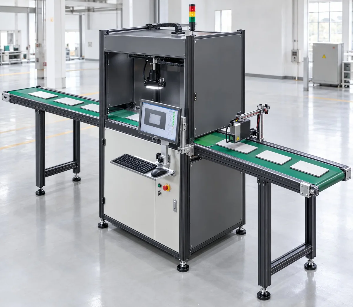
- A microscope-grade optical system is the basis for this type of inspection and must be planned together with the working distance
- For transparent packages, use dark field or coaxial illumination to reveal internal features
- Equipment must suit a clean environment and avoid generating particles and outgassing
OK / NG Judgement
How results are judged and used
| Inspection Status | judgement | Interlocking Action |
|---|---|---|
| All verification items pass | OK | release |
| Missing / deformation / contamination present | NG | Reject and archive |
| Clustered anomalies | Alarm | Alerts upstream process step or environment abnormality |
PLC and Automation Interlocking
How results connect to the production line
It is advisable to retain defect image samples for later process analysis and communication with suppliers.
When interlocking with an automated machine, the timing accuracy of the rejection action directly determines the rejection success rate.
Applicable equipment
Common configuration forms for this type of inspection
Related Solutions
View the corresponding solution by inspection task
Common Question
The Questions Most Often Asked in This Industry
Can micron-level defects be detected?
It depends on the resolution of the optical system and the contrast between the defect and the background. Micron-level inspection requires microscope-grade optical configuration, and the depth of field is extremely shallow, so focusing and flatness requirements are high. It must be validated with actual samples.
Can Standard Industrial Cameras Be Used in a Cleanroom?
The material, surface treatment and heat generation / outgassing of the equipment need to be evaluated. Some scenarios need a dedicated low-particle-emission configuration. This should be confirmed together with the environmental requirements at the solution stage.
For visual inspection in this industry, what needs to be solved first?
The implementation constraints commonly seen in this industry center on: "the inspection objects are extremely small, requiring a high-magnification optical system"; "the depth of field is extremely shallow, so focus stability is demanding"; "reflection and transparent packaging cause imaging interference". These constraints affect both the imaging solution and the cycle-time design. Normally a sample trial is needed to validate before the configuration is finalized.
How does the inspection result interlock with the production line?
It is recommended to keep defect image samples for later process analysis and supplier communication. When interlocking with an automatic machine, the timing accuracy of the rejection action directly determines the rejection success rate.
What Equipment Configuration Does This Type of Inspection Generally Require?
Common forms include: "high-magnification visual inspection cell", "carrier tape / tray inspection station", and "inline inspection system integrated with an automated handler". The specific machine model and quantity depend on the inspection area, minimum defect size, and line cycle time, and must be confirmed against the site conditions.
Which process steps in this industry benefit most from a visual inspection station?
The most common are: "presence/absence and orientation verification of devices in carrier tape / trays"; "lead / solder ball appearance check"; "device marking reading". Which process steps to actually instrument depends on the cost of defects escaping downstream and the cost of rework — the later a defect is found, the higher the cost.
How do we judge whether our product is suitable for visual inspection?
Please provide samples of the parts to be inspected and samples with known defects, and state the minimum detectable feature size and cleanliness class requirements. In general, as long as the criteria can be stated clearly, defects can image clearly and consistently, and the cycle time matches the field of view, the project is feasible.
What inspection accuracy can be achieved?
Accuracy is not a fixed value that holds regardless of conditions. To be added — the minimum detectable size depends on the combination of field of view and camera resolution, and is also affected by illumination, lens and algorithm; the configuration must be derived from your minimum defect size and validated by measurement.
Submit sample testing
Please provide samples of the devices to be inspected and samples with known defects, and state the minimum detectable feature size and cleanliness level requirements.
Submitted successfully
We have received your sample testing request. A solution engineer will contact you within 1 business day via contact you.
Need to assess imaging conditions, defect criteria and cycle time item by item? Go to the Full Requirement Assessment →
Inspection Configuration Based on Your Industry's Products and Cycle Time
Send us photos of the workpiece, the inspection requirement (what to inspect, and the tolerance for escapes and false calls), and the line cycle time, and our solution engineers will recommend the inspection method, optical solution, and interlocking configuration for that industry.