PCB / PCBA
For PCB and PCBA production, providing visual inspection solutions for component presence/absence, position offset, polarity judgement and board-level marking reading.
Industry Production characteristics
How This Industry Produces Determines How Inspection Should Be Done
Visual inspection for PCB / PCBA revolves around two things: first, making the most common defects in this industry image clearly and consistently, and second, integrating the judgement result reliably into the production line. The implementation constraints commonly seen in this industry are "small components are indistinguishable at low resolution" and "dense component areas interfere with each other". Whether defects can be detected consistently depends on the material's optical properties, the minimum defect size and the cycle time, and is subject to the results of a measured sample trial.
The characteristics of PCB / PCBA inspection are Many components, a wide size range and highly structured acceptance criteria. A single board may carry hundreds of components, from 0201 to large connectors.
Because component positions come from the design files, inspection in this industry Naturally suited to being driven by CAD data — converting component coordinates into inspection regions is far more reliable than drawing each region by hand.
Industry Inspection issues
Where problems actually occur on site
- Components missing or offset
- Polarized component installed in reverse
- Wrong part (similar specifications mixed)
- Foreign matter or residue on the pad
- Board-level barcode / QR code must be readable
Typical Inspection Objects
The Most Common Inspection Objects in This Industry
Typical Inspection Task
The judgments to be made on these objects
- Presence/absence and offset verification for each component position
- Polarity marking recognition
- Model differentiation and wrong-material screening
- Board-level marking reading
- Appearance anomaly identification
Vision Inspection Challenges
Implementation constraints specific to this industry
- Small components cannot be resolved at low resolution
- Mutual interference in dense component areas
- Pads and components of the same color (e.g. tin-plated)
- Board silkscreen and traces create a lot of background interference
Choosing the right algorithm
Choose by Acceptance Criteria Form, Not by How Advanced It Is
Multi-Region Rule Algorithm
Judge presence/absence, offset and polarity position by position against the CAD designators
Classification / Mark Recognition
Component type and polarity feature recognition
code reading
Board-level marking reading and traceability
acquisition and light source
Optical conditions set the upper limit of feasibility
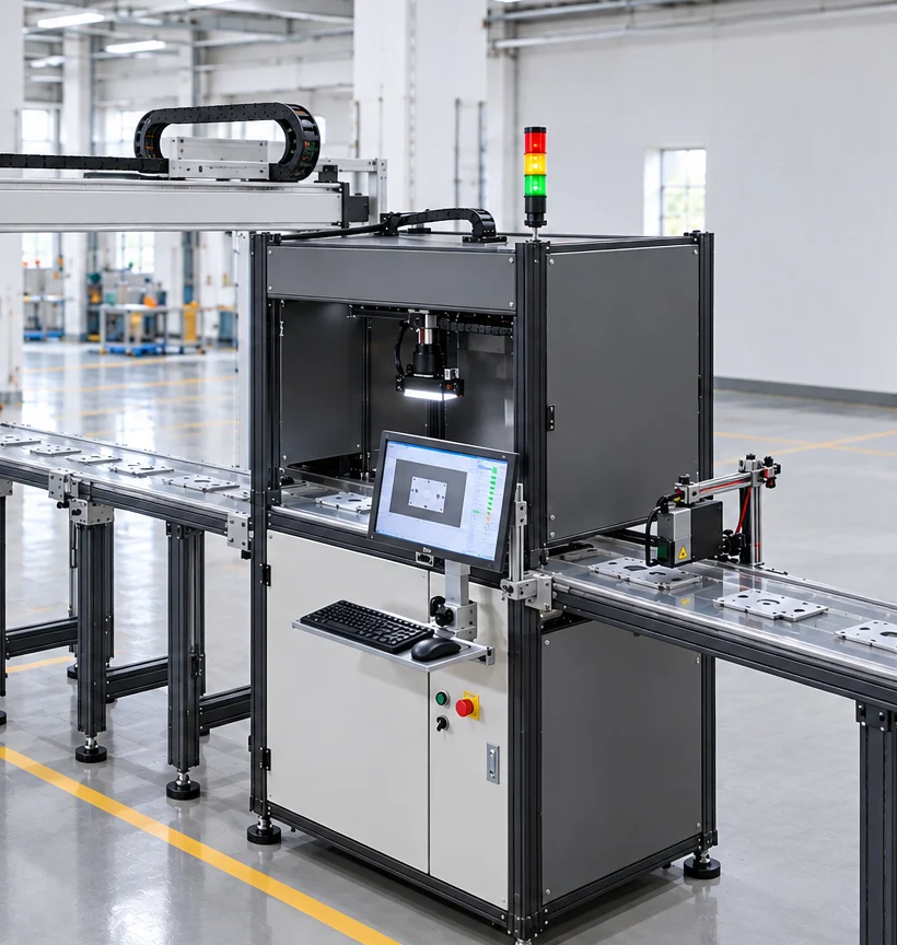
- Coaxial or ring light ensures uniform illumination of components and silkscreen
- For mirror reflection from pads, polarization or diffusion is recommended to reduce it
- Small component inspection needs a low-distortion, high-resolution lens; pay attention to imaging consistency at the edges of the field of view
OK / NG Judgement
How results are judged and used
| Inspection Status | judgement | Interlocking Action |
|---|---|---|
| All components present, positions and polarity correct | OK | release |
| Missing label, offset, or polarity error present | NG | Mark the defect position and route to rework |
| Code Reading Failure | NG | Handle as a missing identifier |
PLC and Automation Interlocking
How results connect to the production line
It is recommended to output the defect Reference Designator output together, so that the rework station can locate the problem directly rather than just receiving an NG signal.
With AOI or MES, inspection results can be bound to the board number to form a traceable record.
Applicable equipment
Common configuration forms for this type of inspection
Related Solutions
View the corresponding solution by inspection task
Common Question
The Questions Most Often Asked in This Industry
Can components as small as 0201 be inspected?
Yes, but a targeted optical configuration is needed: sufficiently high resolution, a low-distortion lens and stable focus. At the same time, the inspection time must be assessed against the cycle time; full inspection of small components usually uses several cameras working in parallel over divided zones.
What is the difference from AOI?
AOI usually covers a complete acceptance criteria system for solder joints and placement quality; the visual inspection in this article focuses more on presence judgements such as presence/absence, position, and polarity. The two are complementary, and the choice depends on the range of acceptance criteria that must be covered.
For visual inspection in this industry, what needs to be solved first?
the implementation constraints commonly seen in this industry center on: "small components are indistinguishable at low resolution"; "components in dense areas interfere with each other"; "pads and components are the same color (such as tinned surfaces)". These constraints affect both the imaging solution and the cycle-time design, and normally a sample trial is needed to validate before the configuration is finalized.
How does the inspection result interlock with the production line?
It is recommended to output the reference designator of the defect as well, so that the rework station can locate it directly rather than only receiving an NG signal. Combined with AOI or MES, inspection results can be bound to the board number to form a traceable record.
What Equipment Configuration Does This Type of Inspection Generally Require?
Common forms include: "EEK-SV5205C industrial vision presence/absence inspection equipment", "high-resolution board-level inspection station", and "multi-camera zoned inspection system". The specific machine model and quantity depend on the inspection area, minimum defect size, and line cycle time, and must be confirmed against the site conditions.
Which process steps in this industry benefit most from a visual inspection station?
The most common is: "per-position verification of component presence/absence and offset"; "polarity mark recognition"; "model differentiation and wrong-material screening". Which process steps to actually instrument depends on the cost of defects escaping downstream and the cost of rework — the later a defect is found, the higher the cost.
How do we judge whether our product is suitable for visual inspection?
Please provide a good board and boards with known defects (missing component / offset / polarity error), and state the smallest component size and the board dimensions. In general, as long as the criteria can be stated clearly, defects can image clearly and consistently, and the cycle time matches the field of view, the project is feasible.
What inspection accuracy can be achieved?
Accuracy is not a fixed value that holds regardless of conditions. To be added — the minimum detectable size depends on the combination of field of view and camera resolution, and is also affected by illumination, lens and algorithm; the configuration must be derived from your minimum defect size and validated by measurement.
Submit sample testing
Please provide a good board and boards with known defects (missing placement / offset / reversed polarity), and state the minimum component size and board dimensions.
Submitted successfully
We have received your sample testing request. A solution engineer will contact you within 1 business day via contact you.
Need to assess imaging conditions, defect criteria and cycle time item by item? Go to the Full Requirement Assessment →
Inspection Configuration Based on Your Industry's Products and Cycle Time
Send us photos of the workpiece, the inspection requirement (what to inspect, and the tolerance for escapes and false calls), and the line cycle time, and our solution engineers will recommend the inspection method, optical solution, and interlocking configuration for that industry.